

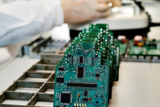
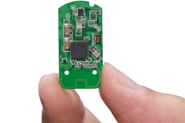
PCB design experts are constantly striving to provide us with the best possible electronic design. And they are constantly working to give us the best possible user experience. However, this implies an increasingly complex design and that is the reason why this process is so interesting to people. The seemingly small board contains a large number of elements that establish flawless cooperation. If you also belong to the group of people who are interested in learning more about the production of PCB boards, you can read all about it below.
Keep in mind that it went through several stages until this level of production was reached. Of course, professionals are just continuing to strive to achieve improvement when it comes to compact design. If you are interested in specific weeds in production, keep reading.
1. The design process
Today, you can notice that almost every company has cooperation with company whose niche is pcb manufacturing. As you can see at www.uetpcb.com such companies do numerous different tasks in order to give you fully functional PCB. As the competition grows, people in their business simply need to focus on some more important things when it comes to functionality, design and product placement. So, certain elements such as the PCB board are left to the professionals and that is a great way to achieve maximum quality. However, people today often opt for this service.
After the cooperation is established and the order is executed, the first step occurs and it refers to the preparation part or the design of the PCB. This step precedes each production, and it involves several steps that must follow all the rules of the process. Basically, these are detailed instructions that will have to be followed from the beginning to the end of the job. Of course, this is followed by an inspection by an engineer and an assessment of the quality of the design. If it meets the criteria, it moves on to the next step and that means the design is converted to a data format.
2. Transition from design to data format
In order for this process to begin, it is important to pay attention to one thing. Uniqueness of tools. The data set must possess this specific element of production. The reason is a customer who can repeat the order after a while and use the same design. Of course, it can happen to make certain changes, but that means that the number of tools also changes. With the established way of functioning in this way, better monitoring is enabled, and that is great news for all customers. Many people use the same number several times.
Continuation of production implies the following. This phase involves the creation of information related to the production steps, product quantity and date. This means that all data that can be linked to the project is analyzed. This includes some drawings, specific requirements, planning, additional instructions, etc. When all this or similar is taken into account, a unique design and process card is obtained. After that, it is possible to identify the project and on that basis provide all the necessary materials for further production. Thus, each project has its own status, but also the operator behind it.
3. Use a list of details for each project
So, engineers are in charge of this step in production. They have a great responsibility that covers several areas. This applies to cleaning, checking and processing data as well as PCB editing, panelization and file routing. When we talk about data cleaning we mean software checking. The engineer must check all the files involved in this as well as the tasks. This is very important to do because it happens that some data is of a different format and then it is necessary to align the layers. Checking and processing data involves comparing the dimensions of the opening and what is in the files. The goal is to make the original drawing plan agree with that.
The PCB editing procedure checks or reviews the files and decides whether it is necessary to make a certain change. For example, it may be necessary to customize tags, data, logo, etc. Finally, the engineer has a responsibility when it comes to panelization. The production panel is the place where the board is placed, and before that is done, it is important that the board is well adjusted. In order for this to be done properly, the whole process is preceded by detailed planning, setting boundaries, determining tools … We must not forget to generate all the files that will be used by the operators on the machines.
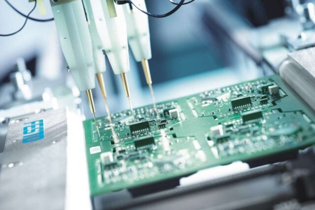
4. Debugging
After engineering works and photo plotting, it is time for optical inspection when it comes to multilayer PCBs. Why is this necessary? Therefore, this inspection needs to be done in order to examine each layer before they are joined. The analysis is very simple, and it is done by comparing the planned design with all the necessary characteristics and the work that has been done. If experts have noticed certain differences during this process, such as excess or deficiency, repairs are done by opening them. This will automatically fix any issues that may later lead to a poor outcome.
However, the simplest approach is to remove some errors immediately in individual layers rather than in the final stage. After all, if the last phase occurs, and the defect has not been removed, it will probably remain until the end of production, because it is difficult to detect with the connecting parts.
5. Applying the surface finish
Although before this process there is a layer that covers everything that is necessary, it is important to apply an additional chemical procedure. It plays a significant role in production because it enables a PCB design that will prevent the consequences of oxidation. Of course, the process will ultimately depend on the surface, which can be different. When all the specific requirements of the board are taken into account, a suitable top coat is obtained. After this, the whole procedure is concluded with an electrical test.
Conclusion:
You have to follow these steps to get perfect PCB. All this happened after the experts got rid of some old ways of connecting, etc. However, when the whole construction is finished, magic is created. Then this little thing becomes an integral part of almost every electronics. We hope we have helped you learn more about this interesting topic.


